Cerebras Completes Series F Funding, Another $250M for $4B Valuation
by Dr. Ian Cutress on November 10, 2021 9:00 AM EST- Posted in
- AI
- Machine Learning
- ML
- Cerebras
- Wafer Scale
- WSE2
- CS-2
_678x452.jpg)
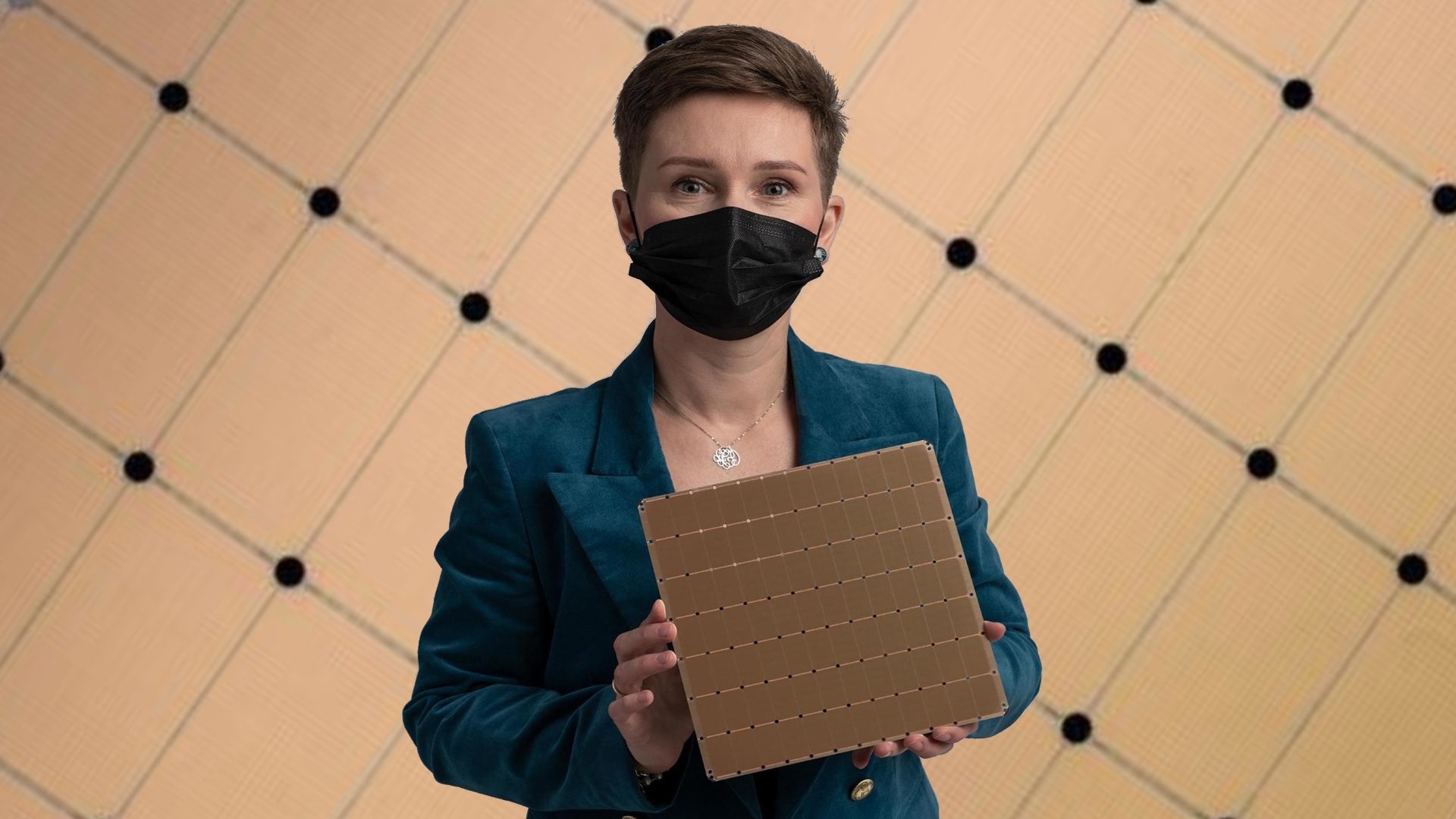
Every once in a while, a startup comes along with something out of left field. In the AI hardware generation, Cerebras holds that title, with their Wafer Scale Engine. The second generation product, built on TSMC 7nm, is a full wafer packed to the brim with cores, memory, and performance. By using patented manufacturing and packaging techniques, a Cerebras CS-2 features a single chip, bigger than your head, with 2.6 trillion transistors. The cost for a CS-2, with appropriate cooling, power, and connectivity, is ‘a few million’ we are told, and Cerebras has customers that include research, oil and gas, pharmaceuticals, and defense – all after the unique proposition that a wafer scale AI engine provides. Today’s news is that Cerebras is still in full startup mode, finishing a Series F funding round.
The new Series F funding round nets the company another $250m in capital, bringing the total raised through venture capital up to $720 million. In speaking to Cerebras ahead of this announcement, we were told that this $250 million was for effectively 6% of the company, bringing the valuation of Cerebras to $4 billion. Compared to Cerebras’ last Series E funding round in 2019, where the company was valued at $2.4 billion, we’re looking at about $800m extra value year on year. This round of funding was led by Alpha Wave Ventures, a partnership between Falcon Edge and Chimera, who are joining Cerebras’ other investors such as Altimeter, Benchmark, Coatue, Eclipse, Moore, and VY.
Cerebras explained to me that it’s best to get a funding round out of the way before you actually need it: we were told that they already had the next 2-3 years funded and planned, and this additional funding round provides some more on top of that, allowing the company to also grow as required. This encompasses not only the next generations of wafer scale (apparently a 5nm tape-out is around $20m), but also the new memory scale-out systems Cerebras announced earlier this year. Currently Cerebras has around 400 employees across four sites (Sunnyvale, Toronto, Tokyo, San Diego), and is looking to expand to 600 by the end of 2022, focusing a lot on engineers and full stack development.
| Cerebras Wafer Scale | |||
| AnandTech | Wafer Scale Engine Gen1 |
Wafer Scale Engine Gen2 |
Increase |
| AI Cores | 400,000 | 850,000 | 2.13x |
| Manufacturing | TSMC 16nm | TSMC 7nm | - |
| Launch Date | August 2019 | Q3 2021 | - |
| Die Size | 46225 mm2 | 46225 mm2 | - |
| Transistors | 1200 billion | 2600 billion | 2.17x |
| (Density) | 25.96 mTr/mm2 | 56.246 mTr/mm2 | 2.17x |
| On-board SRAM | 18 GB | 40 GB | 2.22x |
| Memory Bandwidth | 9 PB/s | 20 PB/s | 2.22x |
| Fabric Bandwidth | 100 Pb/s | 220 Pb/s | 2.22x |
| Cost | $2 million+ | arm+leg | ‽ |
To date Cerebras’ customers have been, in the company’s own words, from markets that have traditionally understood HPC and are looking into the boundary between HPC and AI. This means traditional supercomputer sites, such as Argonne, Lawrence Livermore, and PSC, but also commercial enterprises that have traditionally relied on heavy compute such as pharmaceuticals (AstraZeneca, GSK), medical, and oil and gas. Part of Cerebras roadmap is to expand beyond those ‘traditional’ HPC customers and introduce the technology in other areas, such as the cloud – Cirrascale recently announced a cloud offering based on the latest CS-2.
Coming up soon is the annual Supercomputing conference, where more customers and deployments are likely to be announced.
Related Reading
- Cerebras In The Cloud: Get Your Wafer Scale in an Instance
- Cerebras Unveils Wafer Scale Engine Two (WSE2): 2.6 Trillion Transistors, 100% Yield
- Cerebras Wafer Scale Engine News: DoE Supercomputer Gets 400,000 AI Cores
- 342 Transistors for Every Person In the World: Cerebras 2nd Gen Wafer Scale Engine Teased
- Cerebras’ Wafer Scale Engine Scores a Sale: $5m Buys Two for the Pittsburgh Supercomputing Center
- Hot Chips 2019 Live Blog: Cerebras' 1.2 Trillion Transistor Deep Learning Processor
- Hot Chips 2020 Live Blog: Cerebras WSE Programming
- Hot Chips 2021 Live Blog: Machine Learning (Graphcore, Cerebras, SambaNova, Anton)


24 Comments
View All Comments
austonia - Wednesday, November 10, 2021 - link
i'mma need a bigger motherboard to stick this inbrucethemoose - Wednesday, November 10, 2021 - link
But can it run AND play Crisis?Between Google's DeepMind and Nvidia's interactive demo, I suspect the answer is "Yes."
DougMcC - Wednesday, November 10, 2021 - link
That's not what this kind of thing is for. It can design and implement Crysis.brucethemoose - Wednesday, November 10, 2021 - link
Also, Moore's law is not dead. Cost is simply scaling with performance now.Yojimbo - Wednesday, November 10, 2021 - link
Moore's law will never die as long as we keep redefining what it is. Here is Gordon Moore's paper: https://newsroom.intel.com/wp-content/uploads/site...Gordon Moore made his prediction talking about component costs. Reading what he wrote, he seems to use "components" because he is referencing integrated circuits (ICs) against simple circuits with discrete components. At the time ICs were new. The way I interpret it (I may be wrong, I am not an electrical engineer), we have basically replaced the idea of components in the law with transistors because everything uses ICs today and it's just simpler to talk about. But more importantly he talked about costs. He wrote: "The complexity for minimum component costs has increased at a rate of roughly a factor of two per year (see graph on next page)." But I don't see how that can be true as we are pursuing advanced packaging to lash smaller ICs together. Certainly the current situation doesn't follow his graph, which he seems to interpret as a log-log linear relationship between the number of components per integrated circuit and the cost per component (I believe with an inflection because the rate of change was in flux at the time). In other words, a straight line results from plotting a curve for the logarithm of the number of components per IC against the logarithm of the cost per component for each year and adjoining the minimum cost for each of the curves (if you look at the graph in his paper it will be easier to understand).
Now the cost per component is not decreasing nearly as much as it used to, so the number of components per IC is not increasing as much as it used to. In fact die sizes which used to result in chips that were relatively close to the complexity for minimum component costs are apparently not today, and so chip companies are splitting things into chiplets/tiles. I am sure if we plotted the same type of graph as Moore plotted in his seminal paper for the last 10 years and projected it out 10 years into the future we would see a much different phenomenon than Moore noted in 1965 that led to the formulation of "Moore's Law". The minimum component costs.
By the way, this discussion in Moore's paper was under a section titled "Costs and curves" and immediately preceding the quote I included above he wrote:
"Reduced cost is one of the big attractions of integrated electronics, and the cost advantage continues to increase as the technology evolves toward the production of larger and larger circuit functions on a single semiconductor substrate. For simple circuits, the cost per component is nearly inversely proportional to the number of components, the result of the equivalent piece of semiconductor in the equivalent package containing more components. But as components are added, decreased yields more than compensate for the increased complexity, tending to raise the cost per component. Thus there is a minimum cost at any given time in the evolution of the technology. At present, it is reached when 50 components are used per circuit. But the minimum is rising rapidly while the entire cost curve is falling (see graph below). If we look ahead five years, a plot of costs suggests that the minimum cost per component might be expected in circuits with about 1,000 components per circuit (providing such circuit functions can be produced in moderate quantities.) In 1970, the manufacturing cost per component can be expected to be only a tenth of the present cost."
So he was clearly mostly concerned about cost. From what I remember this idea of cost was a part of "Moore's Law" in the 1990s, and slowly, as that has becomes more and more obviously not holding true, that element of the law has been dropped from it. Another change we seem to have made is to only talk about logic transistor density, whereas Moore was clearly concerned with components which, I would think, should include consideration of SRAM transistor scaling and dark transistors as well. But even if you look at logic transistor density it seems to be under 2x every 2 years now, and so even the very weak formulation of the law seems to be "slowing down".
Yojimbo - Wednesday, November 10, 2021 - link
By the way, the graph on the "next page" he is talking about is labeled "log base 2 of the number of components per integrated function" for the y axis and "year" for the x axis, but from the discussion it's clear he constructed that graph by considering the complexity of minimum component cost for each year.mode_13h - Wednesday, November 10, 2021 - link
I think the Wikipedia page is more informative. There are similar trends which were noted (e.g. Dennard Scaling), and logical consequences (House's 18-month performance doubling period), all of which sort of gets bundled under the heading of Moore's Law (correctly or not).https://en.wikipedia.org/wiki/Moore%27s_law
Yojimbo - Thursday, November 11, 2021 - link
The Wikipedia page on Moore's Law is not very good. It does give Moore's original quote, and it also says "Moore posited a log-linear relationship between device complexity (higher circuit density at reduced cost) and time." but it doesn't really explain the situation well enough to explain what Moore was talking about. Nor does it discuss the practical difference between considering functional components and logic transistor density.mode_13h - Wednesday, November 10, 2021 - link
Anyway, what really matters is looking at the trendlines that we're actually on, and trying to understand when & how those break down. Looking backwards is mostly just for historical interest.Yojimbo - Thursday, November 11, 2021 - link
In other words Moore's Law can continue forever if we forget what it meant in the past and redefine it continually to apply to the future...